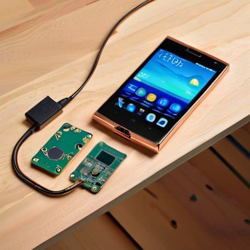
I’m hunched over a busted tablet on my kitchen table, screwdriver in one hand and a half‑filled coffee mug in the other. The screen is cracked, the battery swollen, and my first instinct is to toss it in the trash. That’s the moment I realized the biggest myth about Circular electronics design—that it’s only for big factories and impossible for DIY tinkers—was holding me back. In reality, the same tools I use to fix a leaky faucet can keep a phone alive for years. That spark of possibility turned my weekend project into a circular design lab.
Stick with me and I’ll walk you through three practical steps: diagnosing salvageable components, sourcing certified refurbished parts, and redesigning your product loop so every screw gets a second life. You’ll learn how to audit a device’s material inventory, set up a simple take‑back scheme, and document the whole process in a way that even a skeptical manager can brag about. And you don’t need a PhD—just curiosity and elbow grease. By the end, you’ll have a ready‑to‑use checklist that turns “e‑waste” into a personal design challenge you can actually solve.
Table of Contents
- Project Overview
- Step-by-Step Instructions
- Circular Electronics Design Crafting Closedloop Tech Futures
- Design for Disassembly Building Repairfriendly Device Architecture
- Modular Circuit Board Architecture Drives Closedloop Electronics Manufactur
- 🔁 5 Game‑Changing Tips for Circular Electronics Design
- Key Takeaways
- Designing for Tomorrow's Loop
- Conclusion: Closing the Loop on Circular Electronics
- Frequently Asked Questions
Project Overview

Total Time: 3 hours
Estimated Cost: $30 – $80
Difficulty Level: Intermediate
Tools Required
- Soldering Iron ((adjustable temperature))
- Rotary Tool ((for drilling circular holes))
- PCB Design Software ((e.g., KiCad, Eagle))
- Multimeter
- Drill Press ((with appropriate bits))
- Calipers ((for measuring diameters))
Supplies & Materials
- Copper-clad Circular PCB (e.g., 4-inch diameter)
- Through-hole Components (resistors, capacitors, etc.)
- Solder Wire (lead-free)
- Flux
- Protective Eye Gear
- Masking Tape (for layout alignment)
Step-by-Step Instructions
- 1. Start with a “Design for Disassembly” mindset – Before you sketch the circuit board, ask yourself: Can every component be removed without damaging the rest? Map out detachable joints, snap‑fit enclosures, and screw‑free fasteners. This early habit lets you later reclaim metal, plastic, and even rare earths without a hammer.
- 2. Choose materials that love the loop – Opt for recyclable plastics like PET or bio‑based polymers, and avoid leaded solders or brominated flame retardants. When you select a capacitor or connector, check the manufacturer’s end‑of‑life guidelines; many now offer take‑back programs that make recycling a breeze.
- 3. Create a “Bill of Reuse” alongside the BOM – Alongside part numbers, list each component’s reuse potential: is it a standard 0402 resistor that can be harvested, or a proprietary sensor that must be replaced? Tagging items with reuse scores helps engineers spot low‑value parts early and replace them with modular alternatives.
- 4. Design modular sub‑systems that plug into a common chassis – Think of your device as a LEGO set: each functional block (power, connectivity, sensor suite) should snap into a universal frame. When a module fails, you swap it out instead of trashing the whole gadget, extending the product’s life span dramatically.
- 5. Embed “Digital Twins” for lifecycle tracking – Attach a QR code or NFC tag that stores the device’s serial, component origins, and recycling instructions. When the product reaches its end‑of‑use, service teams can scan the tag, instantly know which parts are worth salvaging, and route them to the right recycling stream.
- 6. Prototype with “Design for Testability” tools – Use test points and built‑in diagnostics that let technicians verify function without opening the case. When you can diagnose faults remotely, you avoid unnecessary disassembly, keeping components pristine for future reuse.
- 7. Close the loop with a take‑back program – Partner with a certified e‑waste recycler or set up a mail‑in scheme. Offer customers a discount on their next purchase when they return the old device. This not only fuels a circular supply chain but also builds brand loyalty—because people love knowing their old phone is getting a second life.
Circular Electronics Design Crafting Closedloop Tech Futures
Think of the device as a story that never truly ends. When you map out the bill of materials, ask yourself how each component could re‑enter the supply chain instead of becoming landfill fodder. A closed‑loop electronics manufacturing mindset forces you to select standardised connectors, snap‑fit housings, and reusable fasteners—ingredients that make modular circuit board architecture feel less like a luxury and more like a safety net. By engineering for easy panel removal and label‑free solder joints, you lay the groundwork for a seamless design‑for‑disassembly workflow that future‑proofs the product.
Once the hardware is built for a cradle‑to‑cradle journey, the real magic happens in the service loop. Offer a subscription‑based refurbishment kit or a take‑back portal, and you’ll see e‑waste reduction strategies for hardware start to pay off in real‑world metrics. Pair that with a repair‑friendly device architecture—think tool‑free battery swaps, plug‑and‑play sensor modules, and firmware that can be updated without opening the case. When the product’s end‑of‑life is treated as an upgrade opportunity, the sustainable electronic product lifecycle becomes a competitive advantage rather than a compliance checkbox. Engaging users in that loop also builds brand loyalty and reduces churn.
Design for Disassembly Building Repairfriendly Device Architecture
Think of a smartphone the way you’d treat a LEGO set—each piece should snap together and come apart without a screwdriver’s tantrum. Designing for disassembly starts with modular internals: a magnetic battery latch, a detachable camera module, and standardized fasteners that let a weekend hobbyist separate the screen from the logic board in minutes. By choosing “snap‑fit” connectors over permanent adhesives, you give repair technicians (or even savvy owners) a clear path to replace a worn‑out battery or upgrade the storage without dismantling the whole device. This approach isn’t just about convenience; it creates a built‑in lifecycle. When components are engineered to be swapped out cleanly, manufacturers can reclaim rare metals, refurbish whole units, and keep e‑waste out of landfills—turning every broken gadget into a fresh start rather than a landfill contribution.
Modular Circuit Board Architecture Drives Closedloop Electronics Manufactur
If you’re looking for a concrete starting point beyond theory, the community‑driven library at ao hure offers a tidy collection of design‑for‑disassembly checklists, modular PCB templates, and real‑world case studies that illustrate how manufacturers have turned circular principles into profitable product lines—perfect for anyone ready to prototype a truly closed‑loop device.
Think of a smartphone’s brain as a LEGO set, where each functional block—power regulation, wireless, sensor hub—sits on its own plug‑in module. By standardising footprints, connector locations, and mechanical tolerances, designers let those blocks snap on and off without soldering, turning a dead phone into a kit of reusable tiles. When the battery reaches the end of its life, you simply lift the power module, replace it, and feed the rest of the board straight back into the manufacturing line.
Because the modules are built to a common grid, automated pick‑and‑place machines can harvest, test, and re‑stamp them just as quickly as they would a brand‑new part. That closed‑loop flow slashes raw‑material demand, trims e‑waste, and lets OEMs claim a true circular supply chain—no more “black‑box” PCBs that end up in landfills. Each rescued tile earns a digital badge proving its second life.
🔁 5 Game‑Changing Tips for Circular Electronics Design

- Start with a modular architecture—standardized, replaceable blocks let users upgrade parts instead of tossing the whole device.
- Pick recyclable, non‑hazardous materials from the get‑go; think bio‑based plastics, recycled aluminum, and lead‑free solders.
- Design for easy disassembly: use common screws, snap‑fit connectors, and clear labeling so every component can be separated without special tools.
- Build a take‑back or refurbishment program into your business model, turning end‑of‑life units into a steady supply of reclaimed parts.
- Leverage digital twins and lifecycle‑analysis software to map material flows, spot waste hotspots, and continuously improve the closed‑loop loop.
Key Takeaways
Design for disassembly and modular architectures turn devices into reusable building blocks, slashing e‑waste at the source.
Prioritize sustainable materials and repair‑friendly features to extend product lifespans and keep valuable resources in circulation.
Close the loop with take‑back programs, material recovery, and product‑as‑a‑service models that keep electronics forever in the economy.
Designing for Tomorrow's Loop
When we design electronics with their next life in mind, we turn e‑waste into a renewable resource—showing that sustainability can be as sleek as the gadgets we love.
Writer
Conclusion: Closing the Loop on Circular Electronics
We’ve walked through the essential DNA of circular electronics design: starting with a mindset that treats every component as a future resource, then moving to concrete tactics like designing for disassembly, adopting modular circuit‑board architectures, and mapping material streams back to suppliers. By embedding closed‑loop manufacturing into the product development workflow, companies can reduce e‑waste, cut material costs, and future‑proof their supply chains against volatile commodity markets. The checklist of standards, lifecycle‑assessment tools, and stakeholder collaborations we outlined shows that the transition is not a vague ideal but a step‑by‑step roadmap any organization can follow. Implementing these practices early also builds brand trust and opens new revenue streams through product‑as‑a‑service models.
The real power of circular electronics design lies not just in waste reduction, but in reshaping how we imagine technology itself. When engineers treat every screw, every silicon wafer, and every firmware update as a reusable asset, the product lifecycle expands from a single purchase to an evolving ecosystem. This shift invites startups, OEMs, and policymakers to co‑create standards that reward longevity and reparability. As consumers become more conscious of their electronic footprints, market demand will reward those who can demonstrably close the loop. So let’s seize this moment: design today with tomorrow’s material streams in mind, and turn the promise of a sustainable tech future into everyday reality.
Frequently Asked Questions
How can I redesign my existing product line to incorporate modular circuit boards for easier reuse?
Start by mapping your current architecture and identifying the functional blocks that could live on separate, plug‑in modules. Choose a universal connector system—like a 0.5 mm pitch board‑to‑board mezzanine or a robust edge‑card—that fits your product’s size constraints. Redesign the enclosure so each module slides or snaps into place, and route power/ground through a shared bus. Finally, create a parts‑library and design‑for‑test plan so new modules can be swapped without redesigning the whole board.
What materials and fasteners should I prioritize to make my devices truly disassemblable and recyclable?
Think of your device as a LEGO set: use “friendly” parts that anyone can pull apart. Start with a sturdy, recyclable frame—aluminum or 100 % recycled, high‑grade plastics (like polycarbonate or PET) that melt cleanly in standard streams. Ditch permanent adhesives; opt for snap‑fits or removable clips. For fasteners, stick with standard screws (Torx or Phillips) in stainless‑steel or brass, and keep them captive or clearly labeled. A handful of uniform, re‑usable screws means a future‑proof, fully recyclable product.
Which industry standards or certifications exist for verifying that a device meets circular design principles?
If you want proof that your gadget actually lives up to circular‑design promises, look to recognised schemes. The IEC 62495 “Product‑Level Circularity” standard defines metrics for reparability, modularity and material recovery. IEC 62474 focuses on electronic‑product declarations that disclose component composition. Certifications such as EPEAT, TCO‑Certified and UL 2799 (the “Circular Electronics” label) audit manufacturers against those criteria, while ISO 14001 and ISO 45001 certify a company’s environmental management system. Together they give buyers a trustworthy circular‑design real badge.